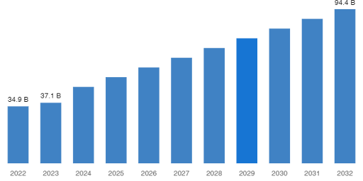
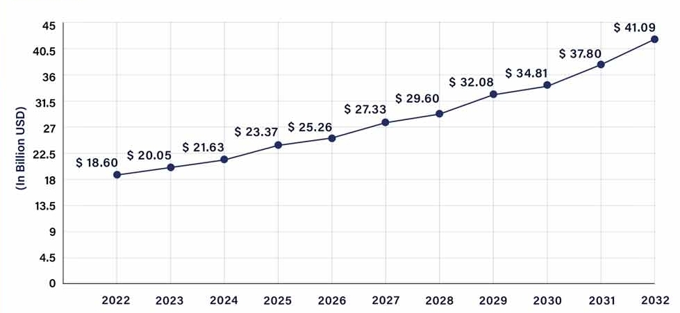
Advanced Packaging Market was valued at over USD 34.5 billion in 2023 and is anticipated to grow at a CAGR of over 10% between 2024 & 2032. The increasing trend toward IoT and AI technologies globally drives growth in the advanced packaging industry. As IoT and AI applications expand, the demand for advanced packaging solutions rises. These technologies often require compact, efficient, and high-performance packaging to ensure optimal functionality. Advanced packaging meets these demands, offering improved thermal management, miniaturization, and enhanced reliability. The surge in demand for device miniaturization is a key driver propelling the advanced packaging market. As consumers and industries alike seek smaller, lighter, and more portable electronic devices, there is an increasing need for advanced packaging solutions that enable the integration of complex components in compact spaces.
So, what exactly is advanced packaging? Advanced packaging refers to a set of sophisticated techniques and technologies used in the semiconductor industry to enhance the performance, functionality, and efficiency of integrated circuits (ICs) and microelectronic devices. Essentially, it’s the process of enclosing semiconductor chips within protective casings and creating the necessary electrical connections, thermal management, and environmental protection to ensure the optimal operation of these chips. The cornerstones of modern electronics were laid with the development of traditional packaging techniques in the latter half of the 20th century. Wire bonding, introduced in the 1950s, remains relevant today. This method uses thin metal wires and solder balls to connect a silicon chip (die) to a printed circuit board (PCB). While space-saving and offering flexibility in connecting distant points on the chip, wire bonding has limitations. It struggles with high temperatures, humidity, and temperature fluctuations, and the sequential bonding process slows down manufacturing. However, with a projected market value of $16 billion by 2031, wire bonding maintains a steady presence.
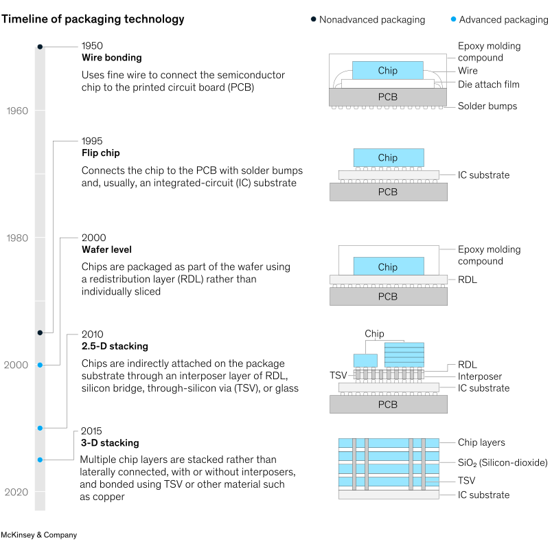
A significant leap forward came in the mid-1990s with flip-chip technology. Here, the die is flipped over, utilizing its entire surface area for connections to the PCB via tiny solder bumps. This innovative approach offers a smaller form factor and faster signal transmission, making devices more compact and efficient. Flip-chip packaging dominates the market due to its cost-effectiveness and widespread use in CPUs, smartphones, and radio-frequency systems. While enabling smaller assemblies and handling higher temperatures, flip chips require very flat mounting surfaces and are difficult to replace. Despite this, the flip-chip market is projected to reach $45 billion by 2030, reflecting a healthy growth rate of 6.3% CAGR.
Wafer-level packaging flips the traditional method on its head. Instead of packaging individual chips, it creates electrical connections and molding on the entire silicon wafer before dicing it with a laser. This results in a smaller package and better heat dissipation due to the use of redistribution layers (RDLs) instead of a substrate between the chip and the PCB. Wafer-level packaging comes in two main flavors: fan-in and fan-out. Fan-in, used for basic applications, routes connections inwards. Fan-out, introduced in 2007, allows for more inputs and outputs while staying thin by extending the RDLs and solder balls beyond the chip size. Within fan-out, core types serve non-demanding applications like automotive and network chips, while high and ultrahigh density cater to mobile and high-performance computing needs. Wafer-level packaging has evolved to stack multiple circuits. This allows for combining logic and memory chips or stacking memory chips. 2.5D stacking takes things a step further, placing chips side-by-side connected by an “interposer.” In 3D stacking, multiple chips are placed face down on top of one another, with or without an interposer.
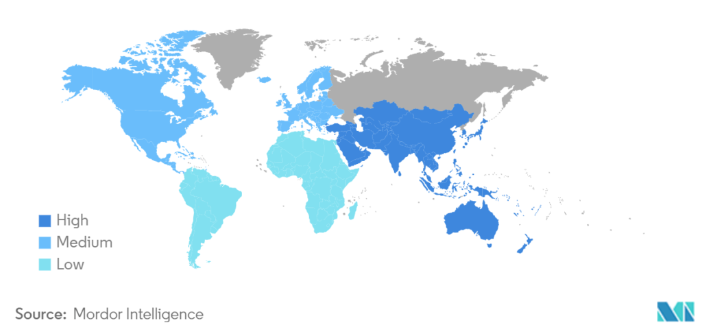
The rise of 5G technology and increasing functionalities in smartphones propel the need for advanced packaging solutions to accommodate complex chip designs. By Region, Asia Pacific held the highest market share in 2022 and is expected to keep its dominance during the forecast period. The surge in demand for consumer electronics, especially in countries like China and South Korea. Asia Pacific dominated the advanced packaging market with a share of over 65% in 2023. The region is expected to witness growth in the market owing to the presence of a strong electronics manufacturing ecosystem, rising demand for feature-rich & compact electronic gadgets, and a spike in the use of 5G technology. Asia Pacific is positioned as a major hub for advanced packaging. The region’s developing market and continuous technological progress create a favorable atmosphere for the development of sophisticated packaging solutions for a range of electronic uses.
Article by: Asst. Prof. Suwan Juntiwasarakij, Ph.D., Senior Editor & MEGA Tech